Project  # 04
Single Digit Up Counter with CMOS  ICs
 

     MORE projects
         

   Get
Price List


Click on picture to enlarge
A completed counter

Click on picture to enlarge
Positions of jumpers (J1, J2) for common cathode 7-segment display 

Click on picture to enlarge
The 7-segment LED display with a red filter (not included) 

OPERATION
 The circuit consists of 2 CMOS ICs : 

(1) CD4518 (Dual decade counters) (datasheet) : this IC contains 2 identical decade counters but only one is used. 
The unused counter has all its inputs grounded (it's important that all unused inputs of a CMOS IC should not be left floating. They are usually tied to circuit ground). The decade counter has 2 inputs : ENABLE & CLOCK.  The ENABLE input (pin 10)  is permanently tied to +Vdd and the CLOCK input (pin 9) is connected to the button switch (S2) so that each time this button is pressed momentarily, a positive clock is generated and the counter outputs (Q4, Q3, Q2, Q1) is incremented by 1.  The following table shows how the outputs change with the input pulses


IC1 outputs
(pin 14, 13, 12, 11)
(1=logic high,  0=logic low)

Displayed character
Q4 |
( 24-1  = 8 )
Q3
( 23-1 = 4  )
Q2
( 22-1 = 2  )
Q1
( 21-1 = 1 )

Reset (Pressing S1)

0 0 0 0 0
Clock input (Pressing S2)
1st pulse
0 0 0 1 1
2nd pulse 0 0 1 0 2
3rd pulse 0 0 1 1 3
4th pulse 0 1 0 0 4
5th pulse 0 1 0 1 5
6th pulse 0 1 1 0 6
7th pulse 0 1 1 1 7
8th pulse 1 0 0 0 8
9th pulse 1 0 0 1 9
10th pulse 0 0 0 0 0
....  and so on 0 0 0 1 1

(2) CD4543
(BCD to 7-segment decoder) (datasheet) : As you may have noticed that the output of the above decade counter is BCD coded and it cannot be used to drive a 7-segment display.  We therefore need another IC (CD4543) to convert the BCD codes to a set of 7 positive signals which individually drives each segment of the display. The segment are labeled  A, B, C, ... , G.  (Note : decimal points LEDs were not used in this project).  A 510Ω  resistor is connected in series with each of the segment output in order to control the brightness & the current of the LEDs. The value of the resistor is selected in such a way that the segment LED's are reasonably bright over the entire supply voltage range of 5 ~ 12V.
 
There are 2 types of displays :
the common cathode &  the common anode.
In this project we have selected the common cathode type.

One special feature of CD4543 decoder is that it is possible to changing the PHASE (or polarity) of the segment outputs voltages by connecting the "PHASE" input (pin 6) to either GND or +Vdd.  Our pcb is designed in such a way that the selection can be done by inserting 2 jumpers at specific locations.  For hobbyists who wish to use a common anode display, please insert the jumpers as shown in this picture  

HOW TO USE 

  1. After the board is completely assembled, connect the circuit to a DC supply of 5 to 12V.  Note that the absolute max supply voltage for CMOS ICs is 15V. A 13V zener diode is included for over-voltage protection. In normal operation, the zener diode is not active. However when the supply voltage exceeds 13V, the diode conducts & prevents Vdd from going over 13V
     
  2. Press the RESET button to clear the counter (display show "0")
    Now press the CLOCK button (S1) once & the counter should read "1".
    Continue to press S2 the counter reading will increase sequentially with every press of the button.
     
  3. The RESET button (S1) : Pressing this button briefly will reset the counter & the display will be "0" 

CONTACT BOUNCING PROBLEM & HOW TO SOLVE IT 
Almost all mechanical switches (such the tactile switches (S1, S2) supplied in this project) have one common problem. i.e. when a switch is depressed (and released), it does not always produce a "clean" pulse. The bouncing of the contact upon switch release produces some "noise" (short pulses known as glitches). These glitches cause the counter to increment more than 1 when S1 is pressed. To overcome this problem, a 0.1 uF capacitor is added (located on the left of S2) to suppress the level of the glitches. Unfortunately, this method is only effective for very short glitches. For longer glitches, we have to look for a better solution.

... More on debouncing --- using micro switch for better result

The structure of a micro switch is quite different from ordinary switch.
There is a small spring inside the switch contact mechanism that causes the contact to open or close with a quick, snapping action. This effectively eliminates the chance of contact bouncing. The pulse produced is thus "clean" & glitch-free. 

 TRY it !!!


Click on picture to view the
schematic

Click on picture to view
components values

Click on picture to view
parts layout
Download  pcb artwork in pdf format

PARTS LIST
(the following components will be included in the package unless otherwise stated)

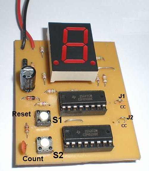
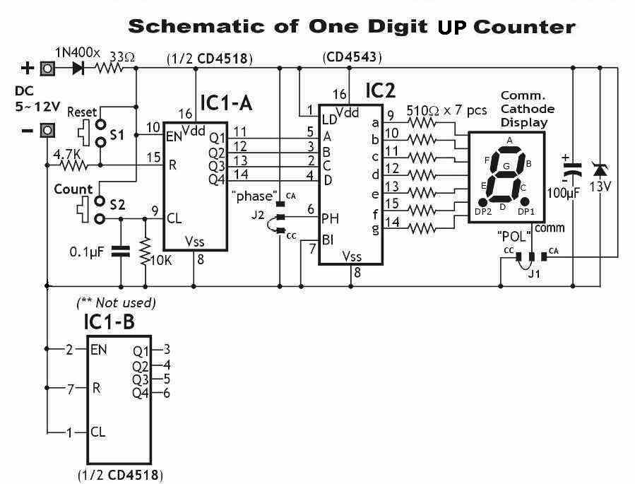
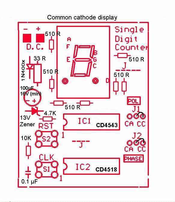
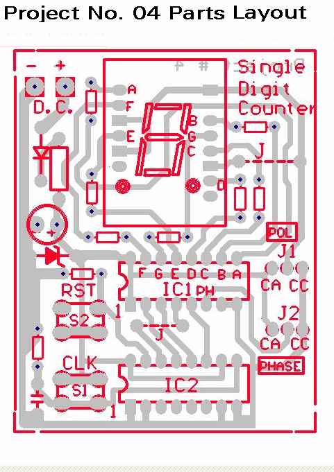
IC-1  ---  CMOS Dual BCD decade counters    Part No. CD4518
IC-2
  ---  CMOS BCD to 7-segment decoder   Part No. CD4543

IC socket, 16-pin  ---------   2 pcs.

Rectifier diode, 1N400x (x=1,...,7)  ---  1 pc.
(for power supply wrong polarity protection)

Zener diode, 13V, 0.5W  ------------ 1 pc.
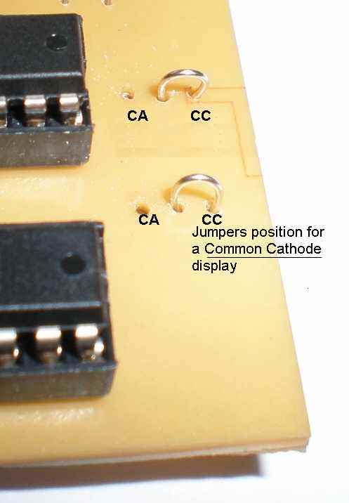
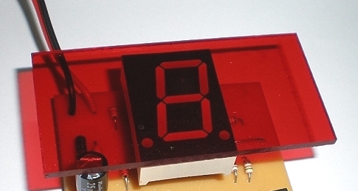
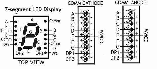
7-segment LED display   ----------- 1 pc.
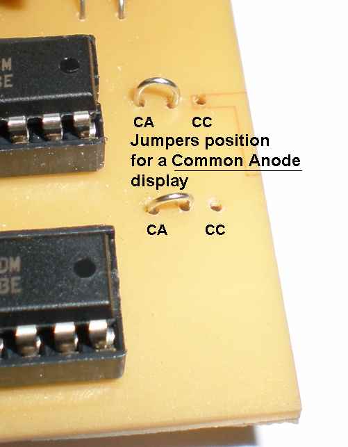
(Common cathode)

510Ω  (1/6 watt) resistor  ------------ 7 pcs.
33Ω    (1/6 or 1/4W watt) resistor  --- 1  pc.
4.7K   (1/6 watt) resistor  ------------ 1  pc.
10K    (1/6 watt) resistor  ------------ 1  pc.

Capacitors :
100 uF, 16V (min) --------  1 pc.  (electrolytic)
0.1 uF   -----------------  1 pc.  (ceramic) (#104, or 100n)

J  (jumpers) -------------  4 pc.  ( any piece of bare wire)


Tact tile switches (S1 and S2) --- 2 pcs
(single contact, normally open, 4-terminal)

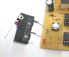
Micro switch  ----------------- 1 pc.
 

Turn pin sockets for mounting

7-segment LED display

1 pc. --- 8-contact socket for right row of display pins 
  
1 pc. --- 6-contact socket for left row of display pins  
 

Download PCB artwork for this project (pdf)
IMPORTANT note on printing the artwork :  Open the pdf file with Acrobat Reader. Use a laser printer to print the artwork on tracing paper *  in true size (i.e., : do not enlarge or shrink the artwork). The printed artwork can be used for direct exposure with UV sensitized pcb such as the Kinsten PP-1530.     
(* tracing paper is the type of translucent  paper used by architect for drawing plans. It's much cheaper than OHP transparency)